


The Hybrid Bonding Wars
How Targeted Sleuthing Revealed a Tactical Long/Short Idea

Chiplets & Hybrid Bonding Background
Moore’s law, the roadmap for the semiconductor industry, is now running up against technological and financial limitations.
The rate of node scaling is slowing.
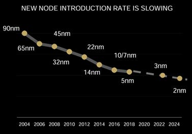
And the cost increase is rising.

To continue improving performance, chip companies have been looking toward ‘chiplets’ architecture, a methodology which disaggregates larger SoC chips into smaller chips; each utilizing only the necessary node for each function.

The challenge for chiplets is how to best reconnect the disaggregated dies in such a way as to have them function together as well as a single monolithic SoC die would.
The best performing solution is a die attach approach called Hybrid Bonding.
Hybrid Bonding allows for the finest bump pitch.
And the highest bandwidth density as measured by I/O count.

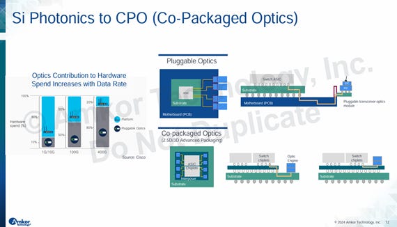
Additional high volume applications for Hybrid Bonding include HBM stacks (moving to 20-high), and Co-Packaged Optics where the EIC and PIC are vertically Hybrid Bonded one on top of the other.
Hybrid Bonding Tool Suppliers:
For Die-Attach tool suppliers, the name of the game has become 'collaboration'. Hybrid Bonding equipment requires a unique partnership between Front-End wafer preparation tools and the Back-End packaging tools to enable maximum throughput at the necessary accuracy levels.
The biggest splash in this space occurred when Applied Materials partnered with BESI, the leading vendor for HB tools. Suss Microtec is also developing a tool with a French die-attach tool maker called SET.
The question now is, are there other potential Front-End or Back-End equipment companies preparing to jump into the race in order to steal the show and take market share from AMAT & BESI?
We believe it is reasonable to see one more major partnership; one which could potentially shift the balance of power when it comes to Hybrid Bonding.
Keep reading with a 7-day free trial
Subscribe to Chips’s Substack to keep reading this post and get 7 days of free access to the full post archives.