


NVLink Fusion Moat, Ajinomoto Guidance, Mobile HBM, C&W April Data Book
Chips & Wafers Weekly Update

NVLink Fusion Moat
Earlier this week at Computex, Jensen revealed a new product: NVLink Fusion, a hardware networking fabric that allows third-party ICs and ASICs to seamlessly integrate and function with Nvidia GPUs and networking solutions. With first-adopters including MediaTek, Marvell, AlChip & more.
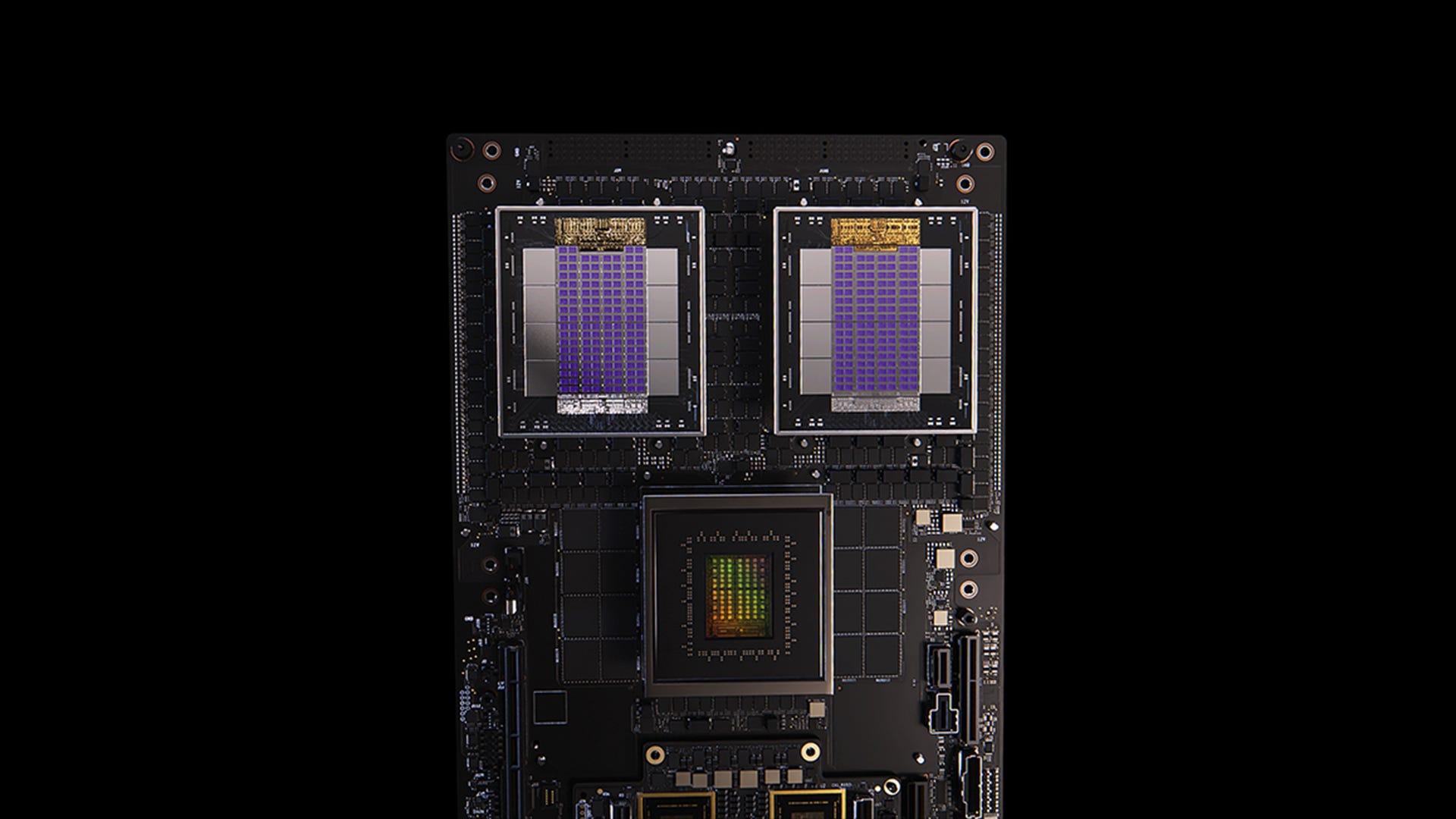
Nvidia has consistently proven over the past decade that it’s ahead of the curve in AI. They were the first to recognize the importance of a software layer above their compute offering (CUDA), the first to understand the need to sell system-level solutions rather than just chips (NVLink-enabled DGX racks), and now they’re taking the next step to fortify their moat.
Every deployer of AI compute has been trying to break away from their Nvidia dependency. After all, who wants to hand over billions of dollars every year for the latest merchant silicon series (GH to GB to VR)? That’s why companies have been racing to develop in-house custom Application-Specific ICs (ASICs)—trying to escape Nvidia’s golden handcuffs and prove their chips are better suited to their unique workloads (à la Google’s TPUs).
Jensen understands he needs to capture those ASIC efforts. How? By creating a product that acts as a force multiplier for every ASIC rack—offering seamless integration between any ASIC and Nvidia GPU, maximizing workload flexibility and efficiency.
Every third party that integrates with NVLink Fusion becomes another node in Nvidia’s growing web—more experience, more data, more optimization potential. And that compounds over time.
This marks the third iteration of Nvidia’s AI moat. Let’s see how it plays out.
But you really have to hand it to Jensen—what a visionary.
Ajinomoto 2025 ABF Guidance
I know what you're asking: What the hell is a food company doing in a semiconductor Substack?
Well, it just so happens that Ajinomoto, known for developing monosodium glutamate (MSG), also manufactures a dielectric insulation film for electronic packaging known as ABF (Ajinomoto Build-Up Film)—and they essentially have a monopoly in this space.
ABF is used in package substrates for CPUs, GPUs, and switches, with the two main end markets being PCs and servers (both AI and general-purpose). So they have a uniquely upstream view of end-market demand.
Interestingly, Ajinomoto just shared its 2025 ABF guidance: +11% YoY. But here’s the kicker—it’s not all about AI:
“Amid the proliferation of AI and growing demand for GenAI servers, firm demand for general-purpose servers and PC replacement demand (including PCs with edge AI) are expected.”
This is important. Most commentary lately around consumer and general-purpose server demand has been weak. But here we have one of the most upstream suppliers suggesting firm demand in these areas.

It's possible a recovery is already underway—and it may come sooner than the market expects.
Mobile HBM – The Edge AI Enabler
There’s been some sentiment in the market that we’re past peak HBM. That doesn’t mean SK Hynix won’t keep growing revenue from HBM, or that we won’t see 16- and 20-high stacks or 8–12 stacks per package—but that the story has already peaked.
Not so fast.
A new report this week suggests that Apple is planning to adopt mobile HBM, enabling serious on-device AI capabilities:
“Apple Intelligence has changed the traditional hardware anatomy inside the iPhone, as the company aims to enhance on-device capabilities. ETNews claims that connecting mobile HBM in the 2027 iPhone's GPU units will allow the devices to achieve just that. The technology, once perfected over time, could allow large language models to run locally on the device without hurting battery life or increasing latency.”
It’s hard to overstate the volume difference between consumer and enterprise applications. If you thought GPU HBM volumes were big, mobile HBM could multiply that demand by orders of magnitude.

The HBM story is not over!
Chips & Wafers April Data Book
Earlier this week, we sent our May Data Book to customers.

When we started Chips & Wafers, we had a simple goal: How can we use objective, quantifiable data to bridge the gap between historical benchmarks and future forecasts?
With that mission in mind, we began aggregating thousands of data points to build a comprehensive library that tracks the semiconductor industry—both from a bird’s-eye view and down to the most granular component level.
We’re proud of what we’ve built. And we believe it offers our customers exactly what they need: Timely and targeted data to guide decision-making.
If you're in the semiconductor space—whether you're an investor or a company—and you're looking for data to drive your strategy, DM us on X, LinkedIn, or email us at
sales@chipsandwafersdata.com for a free demo.
Below we’ll share some slides for our paid subscribers👇
Keep reading with a 7-day free trial
Subscribe to Chips’s Substack to keep reading this post and get 7 days of free access to the full post archives.