Apple WMCM, Renesas & Wolfspeed, TSMC Wafer ASP's & Mainstream... Recovery?
Chips & Wafers Weekly Update
WPM Vs. Die per Wafer - Apple WMCM
A lot of noise recently about AAPL 0.00%↑ adopting CoW-type Advanced Packaging method called WMCM (Wafer-Level Multi-Chip Module). Current research may be missing the forest for the trees. While analysts estimate Apple’s wafer-level multi-chip module (WMCM) packaging could hit 10,000 WPM (wafers per month) by 2026, the tooling requirements to support that scale might be far greater than many realize.
Why? Because in Advanced Packaging, WPM is a misleading metric. Unlike front-end fabs, where WPM maps relatively cleanly to output, back-end packaging throughput depends heavily on the number of dies & packages per wafer—and that’s tied directly to chip size.
For example - 10k WPM for Nvidia Blackwell’s compared to Apple A20’s translates approximately 10x more A20 packages compared to Blackwell. Same WPM, wildly different package output.
Smaller chips like AAPL 0.00%↑‘s iPhone processors mean more packages per wafer, which in turn means more die attach and packaging tool demand per wafer—potentially much more than what’s needed for $NVDA’s large AI server chips using CoWoS.
Bottom line: If Apple’s WMCM plans scale, TSM 0.00%↑ may need significantly more packaging, and inspection tools than what’s currently modeled—making this a possibly underappreciated upside for CoW & test tool vendors (BESI, ASMPT, ONTO, Camtek etc.)
Renesas X Wolfspeed. A Sad Story of Bad Timing
The Silicon Carbide cascade continues. Renesas has restructured its $2.062 billion silicon carbide (SiC) wafer prepayment to Wolfspeed as part of a support agreement tied to Wolfspeed’s planned Chapter 11 restructuring. Under the new terms, Renesas will receive:
$204 million in convertible notes due 2031, convertible into ~13.6% of Wolfspeed’s common stock (pre-dilution)
~38.7% equity stake in Wolfspeed on a non-diluted basis (~17.9% fully diluted)
Warrants equivalent to ~5.0% of fully diluted Wolfspeed shares
The deal also gives Renesas one board seat at Wolfspeed.
In return, Renesas expects to record a non-operating loss of up to ¥250 billion (~$1.65B) in its half-year FY2025 results, but maintains its non-GAAP guidance.
The real story here important to emphasize is that in life, timing is everything. The same is true in semi’s.
WOLF 0.00%↑ was the pioneer of SiC substrates and MOSFET’s and was WAY ahead of the curve here.
But they were too early, and the promised EV revolution was pushed out. This enabled a massive wave of IDM’s to jump into SiC solutions (STM, Infineon, ROHM) and gave the necessary buffer for Chinese firms (SICC, TankeBlue) to flood the SiC substrate market and kill the pricing.
We mentioned in the past how we believe this is a similar phenomenon that is about to hit $BESI and the Hybrid Bonding market. It is unfortunate to observe, but this is the harsh reality in life and in business.
Wafer ASP’s - The Real Chiplet Driver
Earlier this week, SemiAnalysis’s Sravan Kundojjala posted this chart on X:
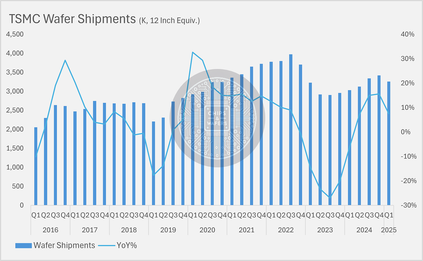
At a high level, the chart illustrates that peak revenue per TSM 0.00%↑ node has climbed significantly—not linearly—starting from the N7 generation onward. While we don’t have official figures on TSMC’s wafer capacity, we do have data on quarterly wafer shipments, which have not grown at the same pace as maximum revenue per node.
So, what’s driving this divergence? Wafer ASPs (average selling prices) are rising much faster than wafer output. This trend is largely due to the stagnation of Moore’s Law, with transistor cost no longer scaling as it once did. In practical terms, this means it’s becoming increasingly expensive to manufacture at each leading-edge node—a major consideration for TSMC’s customers.
The logical workaround is for customers to fabricate different chiplets (tiles) at different process nodes and then integrate them using advanced packaging. This approach improves yield and reduces costs, since only the most performance-critical logic is fabricated at bleeding-edge nodes, while the rest can be produced on more mature, cost-effective processes.
Fortunately for TSMC, they are well-positioned for this shift. Their 2.5D CoWoS platform, along with SoIC and everything in between, is specifically designed to support heterogeneous integration—enabling customers to mix and match different chip types within a single package. Precisely why people are calling Advanced Packaging Moore’s Law 2.0.
Mainstream… Recovering?
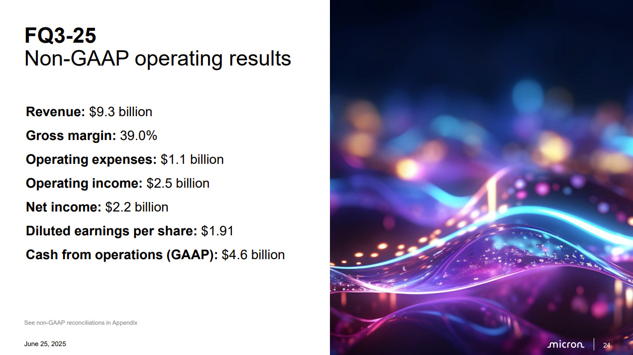
MU 0.00%↑ Reported earnings this week posting formidable results while guiding +15% QoQ.
While most analysts we’re (rightly) focused on HBM commentary, there was a different narrative catching our attention, here are some of the quotes:
"Customers definitely continue to signal a constructive demand environment for the remainder of the calendar year"
"Sequentially, DRAM revenue increased 15% with bit shipments increasing over 20% and prices decreasing in the low single-digit percentage range, primarily due to a higher consumer-oriented revenue mix"
"We expect CY25 industry DRAM bit demand growth to be in the high teens percentage range and industry NAND bit demand growth to be in the low double-digit percentage range"
The comments around consumer demand recovery should start ringing some bells, as the consumer semi segment has been a sleeping giant ever since the COVID super-cycle. And a potential recovery here coupled with secular AI-driven growth could be massive for the industry.
Next week we will be publishing an in-depth report about what we’re seeing vis-à-vis mainstream recovery in our data.
Additionally, we discussed this topic, and demonstrated a number of key indicators, in our most recent Chips & Wafers June Data Book: We offer a one month trial.
That’s a wrap for now. See you next week!
Chips & Wafers Team


